
Our team has done 3D since the turn of the century. It’s been an amazing trip! We’ve seen major advances along the way.
Our fab’s original 3D goal was to stack silicon dies onto silicon wafers with oxide-to-oxide bonds, integrating the layers with metal connections over the sides of the dies. Shortly thereafter, the focus moved to wafer-to-wafer bonding. The biggest challenge was planarity.
Back in the day, manufacturers used CMP (chemical-mechanical polishing) for efficient removal of material with little regard for surface texture. Wafer stacking requires perfectly level, exquisitely smooth surfaces. The fab wizards fine-tuned their CMP process, using less down-force and experimenting with different pads until the wafers reached silky perfection. 2002 saw their first successful wafer stack.

The next step was wafer bonding with metal contacts. Nickel was the fab’s preferred metal, thanks to the fortuitous discovery that nickel and silicon dioxide display similar polishing rates. Nonetheless, some customers prefer copper for its lower cost and greater fabrication availability – so the fab once again tuned its processes. Copper rubs away more quickly than other materials during CMP. Avoiding scooped-out copper areas (“dishing”) is especially tricky during the barrier polish step, where excess barrier metal must be removed without damaging the adjacent copper. Our process experts found ways to tame the dishing and routinely handle either nickel or copper.
3D was now performing beautifully – but way ahead of its time. The stacked chips were tiny, sturdy, fast, and remarkably frugal with power consumption. The problem was that wafer-stacked solutions demanded co-design of all chip layers, specifically crafting them for wafer-stacking. Very few customers had the resources to invest in projects of this magnitude.
But Moore’s Law was running out of steam. Smaller manufacturing nodes became prohibitively expensive and were plagued by poor yields. Chip vendors needed a better way to improve the functionality of their products – but how? The time was right for 2.5D.
2.5D assembly integrates small dies side-by-side on a host substrate such as a wafer or a silicon interposer. The whole assembly is encapsulated in a single package. Somewhat like 3D, the technology offers improved size, weight, and power; unlike 3D, the dies don’t need to be co-designed. Dies can be different sizes, use different nodes, even be built on different wafer materials. In fact, the dies can come from different manufacturers! The host is engineered to accommodate the differences. This versatile and relatively economical solution has quickly moved to the front of chip design. The techniques aren’t quite the same as for 3D, but our 3D expertise gave us a big head start. The fab delivered its first custom 2.5D devices in 2004.
Meanwhile, 3D wafer stacking surges ahead for those big customers that can exploit its unmatched advantages. Cutting-edge projects increasingly call for multi-wafer stacks. To maintain a manageable stack height, each wafer is reduced to gossamer thinness after bonding. Meticulous wafer alignment is also crucial, lest tiny errors accumulate to an unacceptable variance. Our fab has gotten extraordinarily good at all this, skillfully incorporating as many as 20 wafers in a single stack.
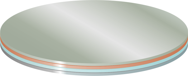
Now the big thing is mixed substrates: stacking wafers that are made of different materials. For example, the industry would love to use more gallium arsenide (GaAs). GaAs makes really speedy components – electrons race through it faster than they can move through silicon – but it’s expensive stuff. Rather than using GaAs throughout an entire device, a GaAs wafer can be stacked with silicon wafers for a whole new level of integration. The difficulty is that the materials have different coefficients of thermal expansion: they expand and contract differently with changes in temperature. The trick is to maintain precise alignment and strong bonds, avoiding buckling or warping. That was an interesting puzzle to solve! But now we’ve stacked silicon with an alphabet soup of materials: GaAs, SiC, GaN, GaSb, InP, LiNbO3, and more.
We’re already looking for the next innovation. At our fab, something new is always coming in the door. Sources change, specifications get rewritten, exotic materials and ideas arise – every project brings some novel twist. And that’s exciting.