ABOUTAn Advanced Packaging Foundry in Three Strategic Locations

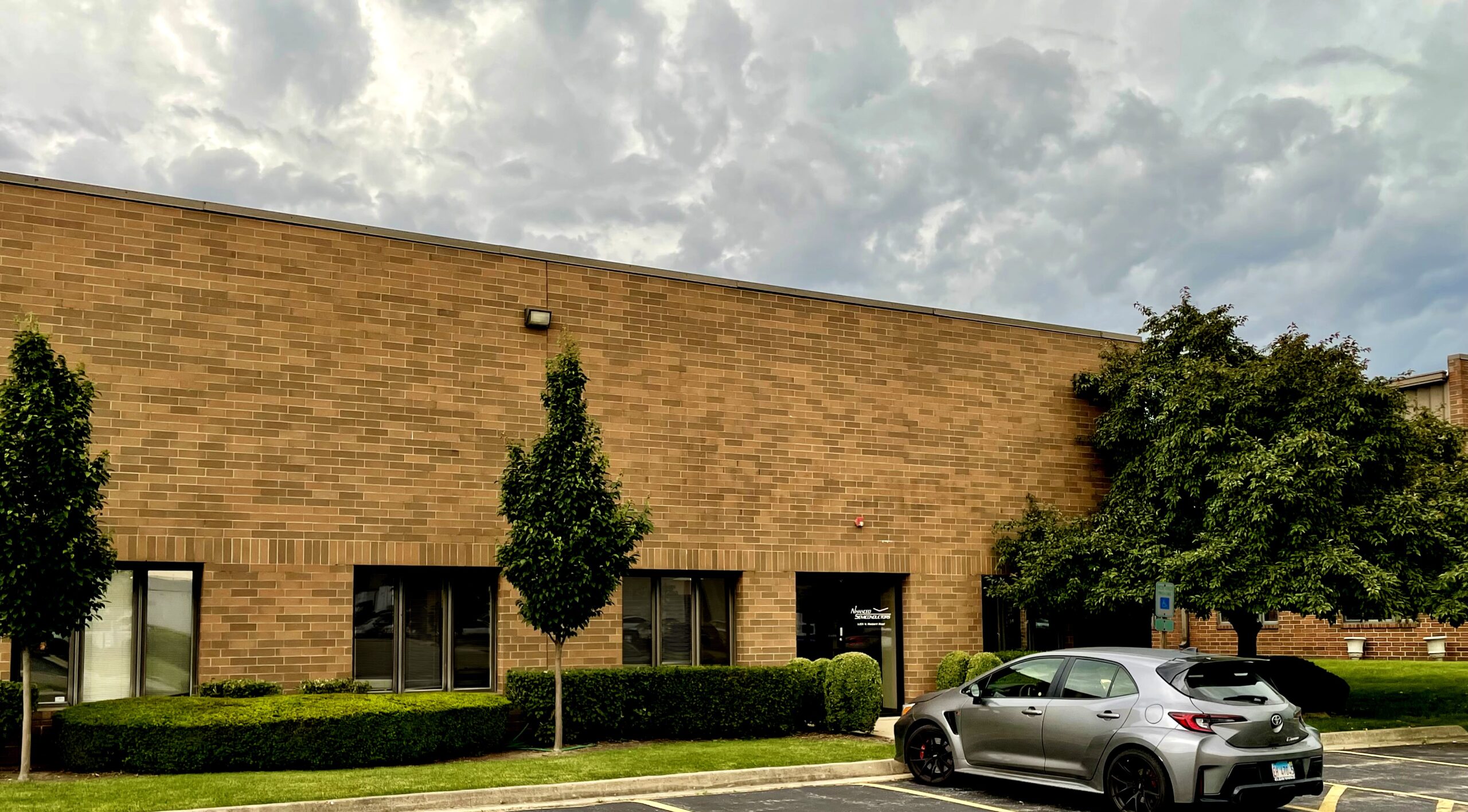
World Headquarters and Design Engineering
1201 N. Raddant Road, Batavia, IL 60510
Known as the “City of Energy,” Batavia gained prominence in the 1800s by manufacturing windmills to power farms across the prairies. Today Batavia boasts Fermilab, a government-sponsored particle physics and accelerator laboratory.
Our headquarters in Batavia is home to our top leadership and our design engineering team. Working under the leadership of 3D pioneer Bob Patti, this versatile crew extends the functionality of advanced ICs in exciting new directions.
Services & Capabilities
- Project management
- Chip, chiplet, and interposer designs
- Circuit redesign for 3D integration
- System-level architecture, definition, specification
- Development of algorithms, drivers, firmware
- Hardware front-end design
- Physical back-end design
- AI systems, embedded software, OS customization
- Schematics, synthesis, verification, emulation
- Mask set generation
- Burn-in boards, load boards, probe cards, QA test programs


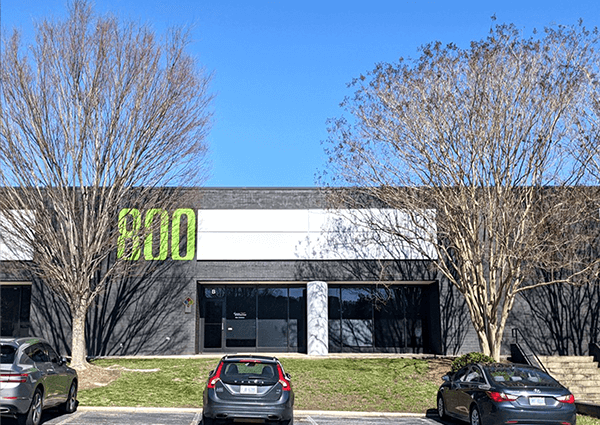
R&D and Prototyping Fab
800 Perimeter Park Drive, Morrisville, NC 27560
Morrisville is in the heart of North Carolina’s Research Triangle, a metropolitan area anchored by Raleigh, Durham, Chapel Hill, and three major research universities.
Our R&D and prototyping fab is ISO 9001:2015 certified for its quality management system as a semiconductor process service provider. The facility’s toolset is ideal for process development and rapid prototyping of 3D-ICs and interposer assemblies. It currently supports wafers up to 200mm including very small specialty wafers.
Services & Capabilities
- Diverse, skilled team of engineers and technicians
- 25,000 sq. ft. facility
- 7,000 sq. ft. cleanroom (Class 100)
- In-house 2.5D/3D technology development
- In-house 2.5D/3D IC prototyping
- Wafer-to-wafer, die-to-wafer, and chiplet-to-interposer bonding
- Hybrid bonding (DBI, DBI Ultra, ZiBond)
- Micro-Transfer Printing (MTP)
- BEOL, both aluminum and copper
- Copper interconnect
- Use of exotic materials
- Photolithography
- Etching
- Thin film deposition
- Surface preparation
- Metalization
- Pick-and-place
- Thinning, CMP, backside processes on thinned surfaces
- Wafer reconstitution
- TSV insertion
- HDI quilt packaging

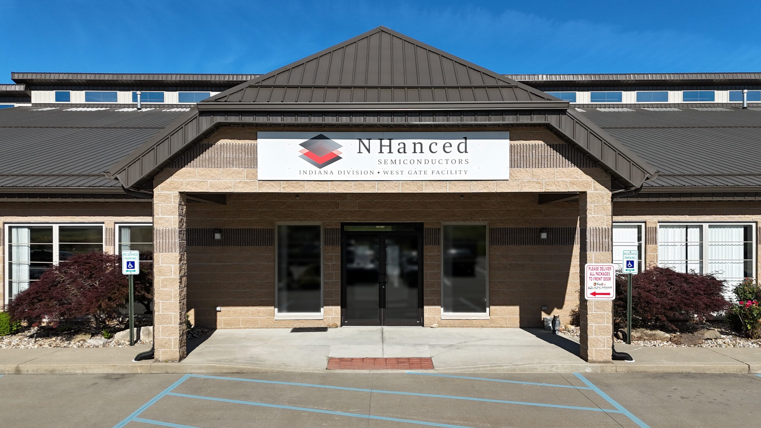
Advanced Package Assembly
14590 Schonberger Drive, Odon, IN 47562
Odon is part of Indiana’s growing semiconductor ecosystem, situated near the US Navy’s Crane facility, the WestGate complex, and several new high-tech ventures.
Purpose-built for the future of low- to mid-volume specialty advanced device production, our Odon package assembly facility came online in November 2023. It supports our Foundry 2.0™ manufacturing model and features two fully-equipped semiconductor cleanrooms.
Services & Capabilities
- Rapidly growing staff and capabilities
- 30,000 sq. ft. facility
- 5,000 sq. ft. cleanroom (Class 100)
- Interposers
- Silicon, glass, fused silica
- Optical and electrical interconnect
- Assembly to substrate
- Photonic assembly
- Solder bumping
- Flip chip assembly
- Thermocompression bonding (TCB)
- Co-packaged optics
- Full prototyping and low-volume assembly on site

