
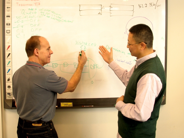
Moving your great idea into successful production takes a talented, creative team:
- Design engineers who can translate brainstorms into brilliant circuitry
- Skilled technical experts for layout and P&R, meticulous simulation, and deep verification
- Hardcore logic gurus to craft embedded software
- Process wizards to transform the design into exquisite, flawless silicon
We are that team.


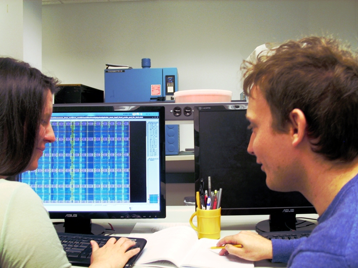
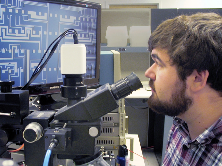
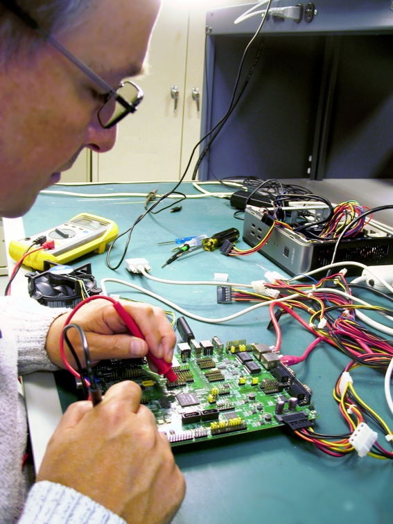
With staff experience averaging more than 20 years, our engineers have solid expertise in high-density, low-power products. They work in deep submicron nodes with a keen eye to cost-size-weight reduction and design sustainability. They have created sensors, FPGAs, SerDes, memory chips (DRAM, MRAM, and RRAM), ASICs, AI systems, and any number of ingenious devices.
This is a versatile crew, with specialties ranging from analog and digital physical designs to low-level system software. Their creations have been successfully realized with 2D, 2.5D, and 3D integration.
Products flow from original concept and initial schematic to top-level mixed-signal verification, all the way through characterization and qualification. Our own fab delivers state-of-the-art prototyping; thermal cycling and probe testing are also performed in-house. Longstanding relationships with vendors and fabs give NHanced an enviable advantage in running a smooth supply chain.
You have the concept – we have the skills. Let’s build something.
Silicon Design Services Menu
- Project Management
- System Level Design:
- Artificial intelligence (AI) systems
- Custom algorithms
- Multi-vendor interfaces
- Architectural Definitions and Specifications
- Software Development:
- Drivers
- Firmware
- Embedded system software
- Operating system customization
- Board bring-up
- Prototype and Production:
- Mask set generation
- Wafer sort, final test, characterization, and QA test program development
- Design of burn-in board
- Load boards, probe cards, socket and package custom tooling
- Product qualification and characterization
- 2.5D interposer design
- 2.5D and 3D stacking (die-on-wafer, wafer-on-wafer)
- Manufacture, assembly, test, and shipment of prototypes
- Hardware Front-End Design:
- Analog / RF Analog / Digital / Mixed Signal
- Schematic design
- VHDL / Verilog / SystemVerilog coding
- Design synthesis
- Functional verification:
- UVM (universal verification methodology)
- Logic simulation
- Formal verification
- Emulation
- Test insertion / test pattern generation
- Physical/Back-End Design:
- Floor planning
- Analog / mixed signal layout (custom and auto)
- Place and route
- .lib timing models (analog)
- Timing closure / Static timing analysis
- Physical verification
- Formal equivalence checking
- Analog / mixed signal verification
- Signal and power integrity analysis
- Post-layout simulation