Benefits of Advanced Packaging for Sensors
- 100% fill factor
- 4-side abuttable devices
- Fast local processing
- Process separation for optimization
Fill Factor
On a classical two-dimensional sensor, the sensing elements share the surface with electronics and wiring. The fill factor is the percentage of the device area that contains active sensing elements. A higher fill factor means higher resolution and less “dead space.”
Moving the design to 3D or 2.5D allows the sensing elements to completely fill the outer layer – 100% fill factor – with wiring and electronics hidden below. The entire surface of the device is active.
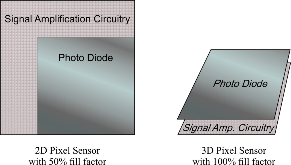
For photo sensors, a 100% fill factor also eliminates the need for micro-lenses.
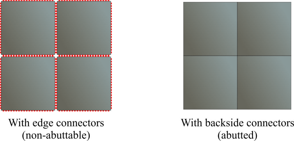
Abuttable Devices
Conventional chips communicate through I/O connections along their edges. These connectors take up some space, leaving gaps between devices in an array.
In a 3D or 2.5D design, I/O connections emerge from the top or bottom of the device. Each device in an array can lie exactly adjacent to other devices on all four edges for a continuous, uninterrupted detection surface.
Local Processing
Designing a device in layers makes room for more functionality. “Smart” sensors include logic and a layer of memory for local data collection and processing. The sensor can analyze and reduce its data before sending it off-chip, deciding which information merits further attention and which should be simply discarded. This has a host of benefits, including:
- Faster frame rate
- Tight focus on areas of interest
- Reduced data transmission
- Less power consumed; less heat generated
Process Separation
Each layer of a 3D device, and each component of a 2.5D device, is built separately. Processing can be fine-tuned to optimize the functionality so that detectors have less leakage, logic has higher speed, etc. Different elements may be built at different nodes, on different wafer types, or even in different foundries.
History and Development
An early driving force for 3D integration was the need for back side illuminated sensors. Thinning the back of the wafer allows more light to come through, but ultra-thin wafers are extremely fragile and difficult to handle. Therefore, in the first incarnation of back side illuminated sensors, the wafer’s front side was bonded to a blank wafer before the back side was thinned. This maintained structural strength in spite of very aggressive thinning.
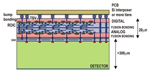
The next generation of sensors attached a layer of logic on the front side of the sensor wafer. This design required vertical data communication through the substrate of the logic wafer using TSVs.
Today, adding a memory layer allows the device to collect and process data in a single chip. The logic layer typically uses more power than the other layers and thus generates more heat, so memory is generally sandwiched between sensor and logic to avoid thermal buildup.
NHanced Builds Advanced Sensors
- Photon imaging chips
- Focal plane arrays (optical and infrared)
- CMOS image sensors
- CCD full frame sensors
- Particle detector arrays
A full suite of processing options for 3D and 2.5D sensors
- Wafer coring (resizing)
- Surface planarization
- Back side stress compensation
- Cleaning and deposition
- Tungsten TSV insertion (back side or via-middle)
- Plasma dicing
- Copper and nickel damascene processes and RDL
- Aluminum RDL and pad metal process
Wafer-to-wafer or die-to-wafer bonding
- Face-to-face, back-to-back, face-to-back
- Chiplet integration on interposers
- More than three active device wafers per stack
- Low temperature bonding
- Oxide bonding
- DBI® (Direct Bond Integration) using copper or nickel
- Micro transfer printing (MTP)
Back side illumination technology
- Silicon thinning: grinding, CMP, dry etch, and wet etch including HNA stop on epi
- IR alignment and printing
- Back side passivation / delta doping / ARC® coating
- Back side metal grid
- Back side pad open
Transfer technology
- Temporary bonding and de-bonding
- Oxide bonding and silicon removal
Interposers
- Thick layer copper damascene
- Silicon, glass, and organic substrates
- Stitched fields (up to full wafer scale)