We Wrote the Playbook on High-Density Advanced Packaging
HYBRID BONDINGDBI® for Die and Wafer Stacking
This is the best technology for stacking dies, wafers, and chiplets.
INTERPOSERSInterposers Enable Chiplets and 2.5D
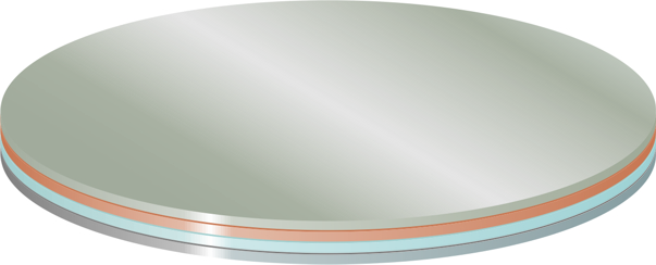
NHanced designs, builds, and implements interposers.
CHIPLETSCreating Mix-and-Match Functionality
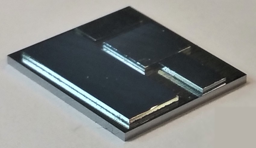
The rising chiplet paradigm enables powerful, flexible designs.

HETEROGENEOUS INTEGRATIONBinding Diverse Components into One Unit
NHanced performs several types of heterogeneous integration.
2.5D INTEGRATIONWhat is 2.5D Integration?
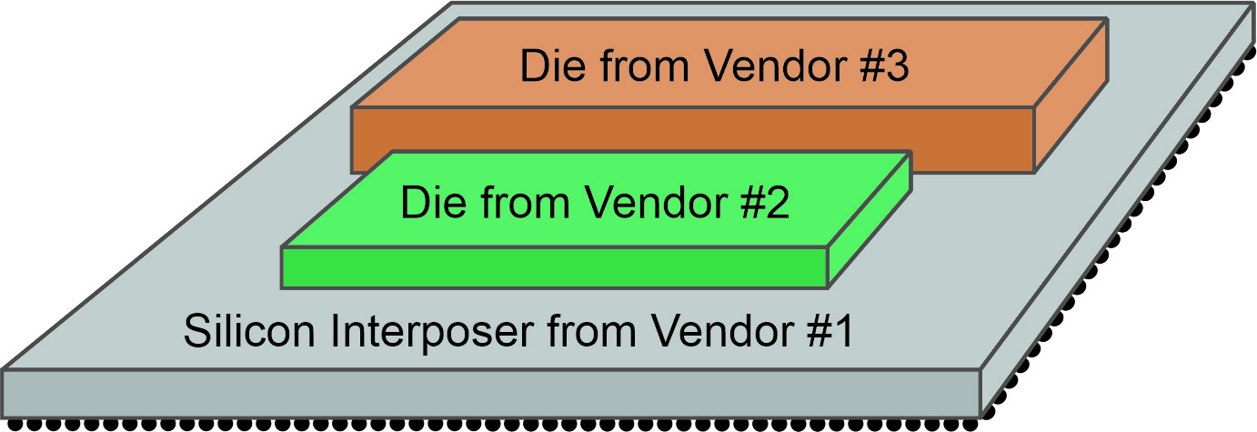
2.5D integration assembles a collection of components side-by-side onto an interposer – a specially designed piece of silicon. The interposer contains circuitry that adapts the components to one another and interconnects them. Some interposers carry devices on both upper and lower surfaces. The on-board circuitry often incorporates TSVs to carry signals vertically through the interposer itself.
2.5D can integrate components that were not designed to be stacked together – off-the-shelf chips, custom chiplets, exotic materials, even a mix of different sources and processing nodes – for true heterogeneous integration.
When Do You Choose 2.5D?
2.5D is an elegant solution for integrating a heterogeneous mix of components to reduce footprint, increase signal speed, and reduce power.
Designing a 2.5D device is much faster and easier than designing a conventional system-on-chip (SoC) because it can use existing components. Modifying the design can be as simple as swapping out one component for another – an enormous benefit in IP reuse and in cost and risk reduction.
Our customers partner with us to tap into an entire 2.5D supply chain, from design and procurement through packaging and test.
Read more about 2.5D technology
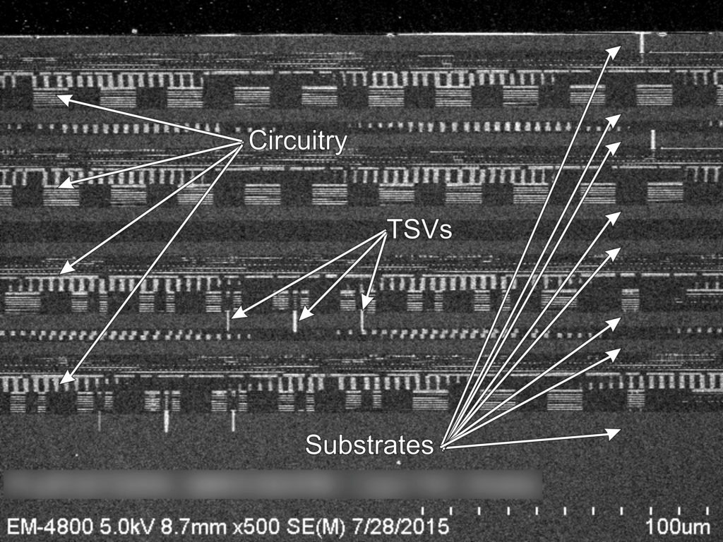
3D INTEGRATIONWhat are 3DICs?
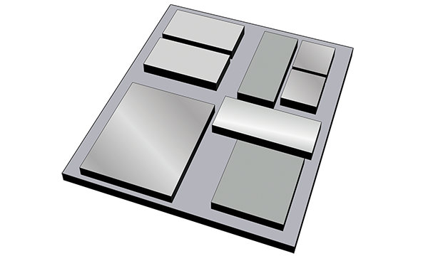
3DICs are multi-layer devices that use through-silicon vias (TSVs) for internal vertical communication. The resulting stack behaves as a single circuit. The extraordinary interconnect density achieved in 3D stacking delivers higher speed at lower power budgets than any other technology.
The layers in a 3DIC must be co-designed for stacking but are built separately, perhaps even in separate fabs. This makes it possible to combine the best of each process, node, and substrate without compromising some components to accommodate others.
When Do You Choose 3DICs?
3DICs deliver the highest density interconnect in the very smallest and thinnest packages. 3D provides even better speed, power, and performance than 2.5D. It is ideal for miniaturized devices such as smartphones and IoT applications where the powerful advantages justify the cost of co-designing the layers.

