NHanced Semiconductors Announces Delivery of the First Next-Generation Hybrid Bonding System from BE Semiconductor Industries
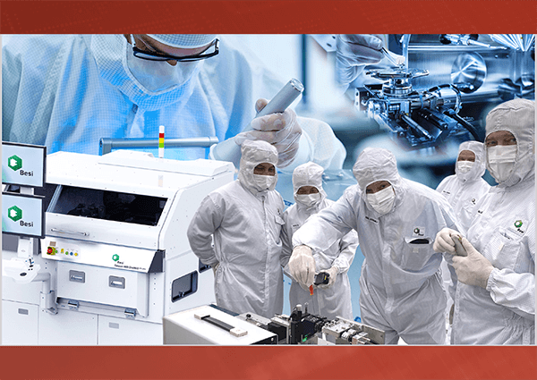
The Besi Datacon 8800 CHAMEO ultra plus advanced hybrid bonding system delivers faster throughput, enhanced accuracy, and superior warpage control for room temperature direct fusion & hybrid bonding processes
MORRISVILLE, NC (MAY 29, 2024) – NHanced Semiconductors, the first U.S.-based pure-play advanced packaging foundry, announced the delivery of the first BE Semiconductor Industries (Besi) next-generation hybrid bonding system to the NHanced advanced packaging facility in Morrisville, NC.
The Besi Datacon 8800 CHAMEO ultra plus is an advanced room temperature hybrid bonding system. It cost-effectively addresses increased demands for performance, speed, accuracy, and warpage control in fine-pitch copper interconnects with submicron pad sizes. Based on Besi’s field-proven Datacon platform, the Datacon 8800 CHAMEO ultra plus hybrid bonder supports room temperature direct fusion bonding of dielectric followed by batch annealing to complete electrical connections, and incorporates state-of-the art vision systems.
“The increased throughput of the new Besi system translates to lower cost for our customers,” said NHanced president Robert Patti. “Even more exciting is the improved yield, which will allow us to handle much larger assemblies economically. I expect to see new products containing dozens of chiplets.”
The new bonding system represents the latest phase in a major investment program by NHanced to amplify and expand its world-class semiconductor and microelectronics ecosystem in the U.S. The company has pioneered a paradigm shift in semiconductor manufacturing that it calls “Foundry 2.0” – applying semiconductor foundry processes and advanced packaging and assembly technologies to dies and chiplets sourced from traditional foundries. The results are customized 3DIC and 2.5D advanced packaging and interposer assemblies. NHanced is the only U.S.-based foundry that can support this manufacturing model.
Photo courtesy of Besi.
About NHanced Semiconductors, Inc.
NHanced Semiconductors is the first pure-play advanced packaging foundry in the US, specializing in leading-edge BEoL semiconductor technologies. Its capabilities include chiplets, 3DICs, silicon interposers, 2.5D, additive silicon manufacturing, photonics, microfluidics, and other innovative technologies. The foundry works with both standard and non-standard substrates, III‑V compound semiconductors, and many specialized materials.
Headquartered in Illinois, NHanced has a development and manufacturing facility near Research Triangle Park, NC, performing small volume manufacturing, in-house process development, and customer prototyping, and an advanced packaging and assembly facility in Odon, IN. For more information, please visit: https://nhanced-semi.com/
NHanced media contact:
Gretchen Patti, NHanced Semiconductors
331-701-7070 x109
gpatti@NHanced-semi.com
###


