
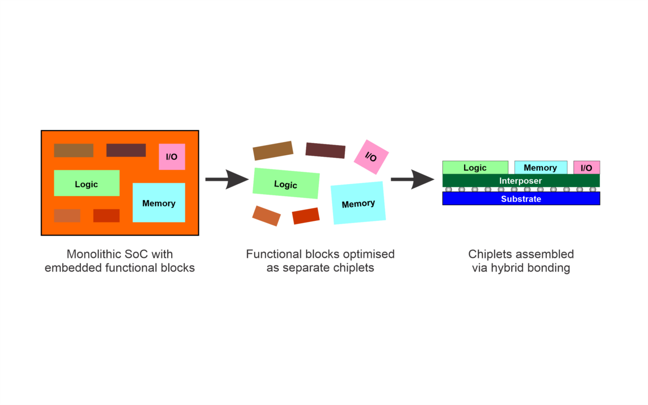
As semiconductor scaling slows and system complexity accelerates, the industry is shifting from monolithic system-on-chip (SoC) designs to chiplet-based architectures. This transition is not simply architectural. It raises the bar for advanced packaging — and hybrid bonding has emerged as a cornerstone technology.
Electronics Weekly explores this topic in an article contributed by our own Chuck Woychik: Chiplet architecture is the future of electronics packaging