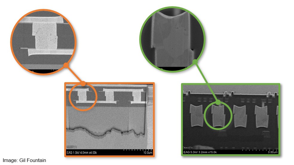
Cross-sections show tiny, precise interconnects created by hybrid bonding
Hybrid bonding enables 3D-like chips, advanced packages and other products with ultra-fine interconnects
By Mark LaPedus
“NHanced Semiconductors, a U.S.-based pure-play advanced packaging foundry, is expanding its efforts in the hybrid bonding market.
NHanced has recently taken delivery of an advanced hybrid bonding system from BE Semiconductor Industries (Besi), a supplier of assembly equipment based in Duiven, the Netherlands. The new hybrid bonding system will expand NHanced’s efforts in the advanced packaging market.
Based in Batavia, Illinois, NHanced provides a wide range of packaging services for customers. The company’s packaging capabilities include 2.5D technologies, 3D-ICs, chiplets, microfluidics, photonics, silicon interposers and others.
For years, NHanced has also developed and shipped various products using a technology called hybrid bonding. Generally, hybrid bonding enables 3D-like chips, advanced packages and other products with ultra-fine interconnects…”