At NHanced we’re passionate about inspiring the next generation of tech innovators. Tours of our manufacturing facility in Odon Indiana, located next to NSWC Crane, offer high school and college students a unique look into advanced semiconductor packaging and the incredible opportunities in this dynamic industry.
“We are thrilled to collaborate with local future talent to revitalize manufacturing in the Midwest,” says Emily Klaski, Process Engineer and Technical Assistant to the President of NHanced Indiana Division. “We’re committed to strengthening the local ecosystem and partnering with our fellow Hoosiers.”
These tours aim to bridge education and industry, connecting classroom learning to industry applications. They are crafted to ignite interest in semiconductor manufacturing, showcase cutting-edge technologies, and highlight the many career possibilities.
The immersive tour features:
- Meeting the Experts: Students engage with our skilled professionals, learning about their career journeys and diverse roles, from process engineers to facilities maintenance technicians.
- Behind-the-Scenes Access: Participants get close-up views of our production facility and its specialized equipment, such as a fountain electroplater and a plasma-enhanced chemical vapor deposition tool.
- Career Guidance: We provide information about potential career paths and internships, helping students envision their future in Indiana’s growing semiconductor industry.
Students are particularly captivated by:
- The Cleanroom Environment: Seeing the stringent protocols and specialized gear required for chip manufacturing.
- Advanced Packaging Technologies: Observing techniques such as chemical-mechanical polishing of silicon wafers.
- The Scale of Operations: Understanding how microscopic processes translate into global impact.
These tangible experiences can spark a lifelong passion for technology and innovation. Students see first-hand how classroom concepts in physics, chemistry, and engineering apply to real-world manufacturing.
Benefits for students:
- Exposure to cutting-edge technologies
- Introduction to potential career paths
- Networking opportunities with industry professionals
We receive enthusiastic feedback from participants, with many expressing newfound interest in semiconductor manufacturing. By maintaining strong partnerships with local colleges, we aim to nurture and develop future talent, ensuring a vibrant and skilled workforce for years to come.
Benefits for NHanced and the Indiana tech sector:
- Early engagement with potential future employees
- Increased local awareness of our industry
- Strengthening of the local STEM ecosystem
- Accelerated workforce development
In short, our student tours enhance the position of our region – the Silicon Crossroads of the Midwest – as a vibrant hub of semiconductor innovation.
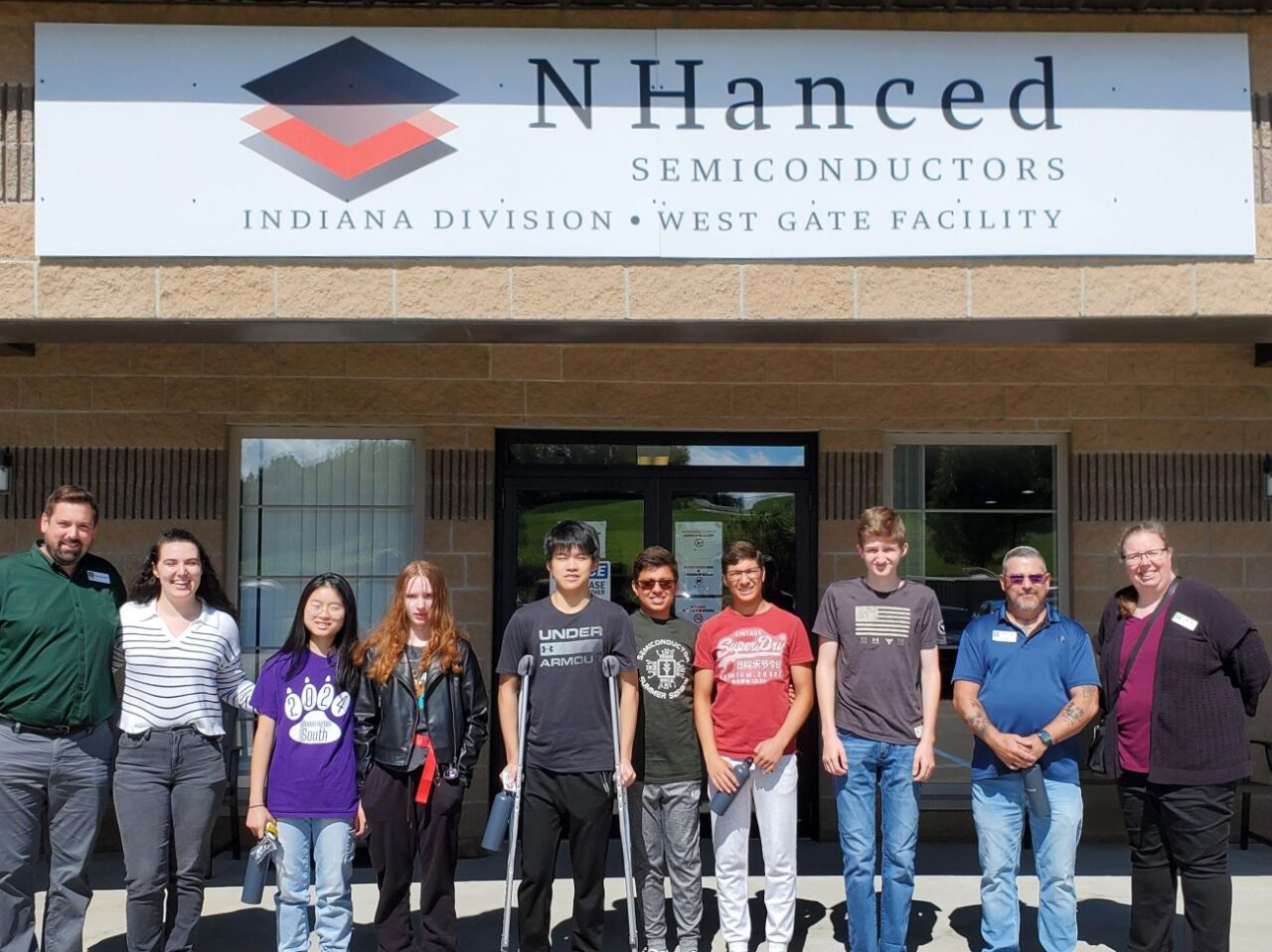
Feedback from Ivy Tech
A recent tour brought students from Ivy Tech Community College (shown in photo) to the NHanced fab. Michael Waterford, Employer Liaison for Ivy Tech, says: “The tour at NHanced Semiconductors was a transformative experience for our students. It not only enhanced their understanding of the semiconductor fabrication process but also ignited a passion for microelectronics. The insights and real-world applications they encountered have inspired many to pursue careers in this innovative industry. We are grateful to NHanced, and especially Emily Klaski, for caring about the future of Indiana’s workforce and sharing this invaluable experience.”
Looking ahead
As we look to the future of our manufacturing sites, we’re excited about the possibilities for our tour program. By exhibiting the latest advancements in semiconductor technology, such as 3D packaging and silicon photonics, we encourage students to consider a personal role in this rapidly evolving field.
Join us for a Tour
Interested in experiencing advanced semiconductor packaging manufacturing firsthand? Whether you’re a student curious about microelectronics, an educator looking to inspire your class, or an industry professional, we’d love to show you around our state-of-the-art facilities.
For more information about the facility tours or to arrange a visit, email us at tours@nhanced-semi.com
At NHanced Semiconductors, we’re dedicated to advancing both technology and education. Our doors are open – come discover the fascinating world of advanced semiconductor manufacturing with us!