What is 2.5D?
2.5D, often referred to as interposer technology, is a sophisticated approach to integrating multiple electronic components within a single package. This method arranges components side-by-side on a shared base — the interposer — which facilitates connectivity. This advanced packaging technique blends the simplicity of 2D with many of the technical innovations of 3D integration.
Components, typically produced independently, are assembled on the interposer, a substrate equipped with TSVs (through-silicon vias) for enhanced signal transmission. This allows for a compact assembly, often capable of supporting components on both its surfaces, that will behave as if it were a single integrated circuit.
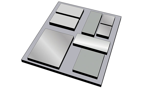
There may be any number of separate components on the interposer. Each may be a standard 2D die, a 3D IC, a specialized “chiplet” designed for 2.5D assembly, or any other type of integrated circuit. The entire assembly is then encapsulated in a single package (Figure 1).

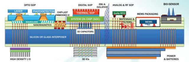
Figure 2 illustrates the far-ranging possibilities of 2.5D integration.
Advantages of 2.5D Packaging
In conventional 2D circuits, each die is packaged separately. The packaged chips are laid out on a circuit board and connected to one another with tiny wires (Figure 3).
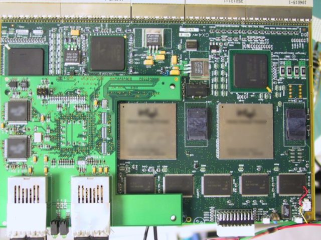
Figure 3: A typical circuit board comprising 2D electronic circuits.
Compared to these conventional circuits, 2.5D technology offers a significant leap in efficiency:
- Footprint: 2.5D remarkably reduces the spatial requirements, potentially matching the size of a single conventional 2D chip while containing multiple components. This space-saving advantage is crucial for devices where compactness is key.
- Speed: The proximity of components on the interposer ensures faster signal transmission, outpacing traditional circuit boards and approaching the efficiency of 3D IC advanced packaging. This is especially beneficial for high-performance computing and telecommunications applications.
- Power Efficiency: By shortening connection lengths and omitting ESD protection among closely packed components, 2.5D assemblies significantly reduce power consumption. This efficiency is vital for portable and battery-operated applications, where power conservation is paramount.
- Simplified Integration: Unlike 3D ICs, 2.5D assemblies can integrate existing circuits without the need for redesign, streamlining the development process. This simplification allows for quicker time-to-market and reduced development costs.
- Heterogeneous Integration: Assembling components on an interposer allows diverse technologies to coexist within a single package, with interfaces facilitated by the interposer itself. This integrative capability enables the combination of analog, digital, and RF functions within the same package. Components may be from different sources, made of different materials, or built in different processes. These flexible, eclectic combinations optimize performance and functionality.
In short, interposer technology represents a middle ground in the spectrum of packaging technologies. It is more complex and costly than traditional 2D packaging but doesn’t quite reach the compactness or performance capabilities of full 3D integration. This balance has led to its description as “2.5D,” a whimsical term that captures its position between the two paradigms of electronic packaging. Today’s engineers widely adopt 2.5D as an elegant, workable solution for a range of applications.
Challenges and Solutions in 2.5D Implementation
While 2.5D technology presents a middle ground between traditional and 3D packaging, its implementation is not without challenges.
Despite the LEGO®-like diagrams in so many presentations, the high complexity of designing an interposer to accommodate a variety of components requires a deep understanding of multiple technologies and creative engineering solutions.
For example, the perfect design may combine off-the-shelf chips and custom chiplets, standard CMOS and exotic materials, and perhaps even a mix of different processing nodes. The underlying interposer is a high-tech marvel. Seamlessly integrating the several elements calls for experience and creativity — and that’s where we shine.
NHanced stands at the forefront of 2.5D and 3D advanced packaging, offering end-to-end services from design through packaging and testing. Our expertise in custom chiplet and interposer designs, combined with our mastery over the 2.5D packaging process, positions us as your ideal partner for embracing 2.5/3D packaging solutions.
NHanced manages the entire 2.5D supply chain, from design and procurement through packaging and test, and is ready to transform your vision into reality. Are you ready to NHance your product? Contact us today.