Leading-Edge Facility Opens in Odon, Indiana
NHanced Semiconductors Opens Leading-Edge Advanced Package Assembly Facility, Reinforcing Indiana’s Position as a Major Semiconductor Hub
January 22, 2024 – Odon, Indiana
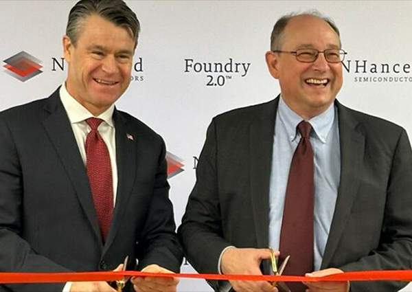
U.S. Senator Todd Young (R-IN) and NHanced Semiconductors President Robert Patti, at the ribbon-cutting at the Odon facility, announce new advanced semiconductor packaging capabilities, making the state a key player in Indiana’s high-tech future
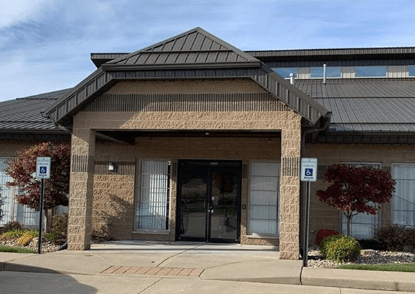
ODON, IN (JANUARY 22, 2024) – NHanced Semiconductors is a US-based pure-play advanced packaging foundry specializing in leading-edge technologies. NHanced president Robert Patti was joined by U.S. Senator Todd Young (R-IN); Andrea Richter-Garry, senior VP of the Indiana Economic Development Corporation (IEDC), representing Indiana Governor Eric Holcomb; and Dr. Kyle Werner, NSWC Crane Deputy Technical Director, at the ribbon-cutting ceremony for its NHanced WestGate Facility, a multimillion-dollar advanced package assembly center, on January 19. This represents the latest phase of a major investment program by NHanced to establish a world-class semiconductor and microelectronics ecosystem in Indiana.
Speaking at the NHanced WestGate Facility, Senator Young said, “Innovative companies like NHanced are not only providing good jobs, they are keeping us safe and secure by making technological advancements with military applications.” Senator Young continued, noting that the federal CHIPS and Science Act was passed, in part, to encourage investments like this: “Indiana is emerging as a key player in our high-tech future, and we’re grateful for the investment NHanced is making in Hoosiers.”
According to Patti, “This is our first step in bringing advanced semiconductor packaging to Indiana. Our final aim, when the WestGate One complex is complete, is to deliver full Foundry 2.0 services to fulfill the needs of the US Government.”
Representing Governor Holcomb’s office, Andrea Richter-Garry, Senior Vice President of Global Strategy and Engagement at the Indiana Economic Development Corporation said, “Indiana is taking bold action to put our state at the forefront of critical innovations and key industries in order to create a more prosperous future for Hoosiers.” She added. “And we’ve become a destination of choice for the semiconductor industry. Our state offers a robust tech ecosystem to support semiconductor manufacturing and development throughout all levels of the microelectronics value chain.”
“NSWC Crane is delighted to help kick off the important semiconductor packaging work that will happen at NHanced and the WestGate One complex,” said Dr. Kyle Werner, NSWC Crane Deputy Technical Director. “Advanced semiconductor technology is central to supporting our nation’s Nuclear Triad and priority nuclear modernization efforts underway. Working with NHanced, and so many others, the Innovation Ecosystem at NSWC Crane accelerates the development of critical solutions to advance Warfighter capabilities that keep our nation safe. A special thank you to all partners involved and NSWC Crane very much looks forward for what’s to come,” he said.
The new Odon NHanced facility features two state-of-the art cleanrooms – one will house the company’s semiconductor advanced package assembly line and the other is planned for process development and training, specifically for the NHanced foundry in Bloomington, expected to open later this year.
The Odon facility is designed as part of WestGate One – a multi-company complex that will be the first semiconductor foundry in the US built specifically for advanced package manufacturing. NHanced and several other semiconductor companies will occupy the ten-acre public-private development adjacent to the Crane Naval Surface Warfare Center, with future partnerships expected with industry, government, and educational institutions.
The combined companies of WestGate One are expected to create more than 500 high-tech jobs with average salaries of more than $100K/year.
Both the companies and the governments have announced commitments to support training initiatives for the new workforce. NHanced is already working with Indiana universities and trade schools to build the workforce; future plans include STEM efforts for K-12 education.
Photo caption: (left to right) Andrea Richter-Garry, senior IEDC VP, representing Indiana Governor Eric Holcomb; U.S. Senator Todd Young (R-IN); Nhanced Semiconductors President Robert Patti; and Dr. Kyle Werner, NSWC Crane Deputy Technical Director
About NHanced Semiconductors, Inc.
NHanced Semiconductors is the first pure-play advanced packaging foundry in the US, specializing in leading-edge BEoL semiconductor technologies including chiplets, 3D-ICs, silicon interposers, 2.5D, additive silicon manufacturing, photonics, microfluidics, and other innovative technologies. The foundry works with both standard and non-standard substrates, III‑V compound semiconductors, and many specialized materials.
Headquartered in Illinois, NHanced also has a development and manufacturing facility near Research Triangle Park, NC, performing small volume manufacturing, in-house process development, and customer prototyping.
About NSWC Crane
NSWC Crane is a naval laboratory and a field activity of Naval Sea Systems Command (NAVSEA) with mission areas in Expeditionary Warfare, Strategic Missions, and Electromagnetic Warfare. The warfare center is responsible for multi-domain, multi- spectral, full life cycle support of technologies and systems enhancing capability to today’s Warfighter.
Local contact:
Marcy Medina, NHanced Semiconductors
(331) 701-7070
mmedina@nhanced-semi.com
Media contact:
Chris Burke, BtB Marketing Communications
(919) 637-3510
Chris.burke@btbmarketing.com
###
Odon Commissioning PR Technical Media Addendum
NHanced Semiconductors, Inc. is the first pure-play advanced packaging foundry in the US. As a manufacturing innovator, it has extensive expertise in cutting-edge semiconductor technologies, including the concept of Foundry 2.0™– applying the semiconductor foundry processes of advanced packaging to create system-level solutions that minimize costs and risks while delivering superior performance and faster cycle times. Foundry 2.0 opens access to smaller market segments by performing cost-effective high-mix manufacturing at low and medium volumes.
NHanced’s Foundry 2.0™ manufacturing model uses dies and chiplets sourced from traditional high-volume semiconductor foundries. It integrates them in novel combinations with through-silicon vias, glass or silicon interposers, non-silicon materials, compound semiconductors, passive devices, and other elements. The resulting products are sophisticated, strongly differentiated advanced package assemblies such as 3D ICs (vertical multi-level stacks of dies) and 2.5D ICs (dies arranged on interposers in planar or stacked configurations).
Advanced packaging technologies employ heterogeneous integration, additive silicon manufacturing, photonics, microfluidics, III-V compound semiconductors, and other high-end solutions that support large scale electrification, 5G wireless communications, and widespread deployment of artificial intelligence (AI) for applications in medical, industrial, and aerospace & defense.
New Odon Plant to Add Assembly Capacity and Support Other NHanced Facilities
The new Odon facility will handle mid-volume advanced package assembly and will support NHanced’s adjacent facility in the future (2026) WestGate One complex. The Odon facility features two cleanrooms for semiconductor assembly and for training staff to be employed at NHanced’s future 170,000 square foot foundry in Bloomington, Indiana.
According to NHanced, the conventional high-volume outsourced semiconductor assembly and test (OSAT) companies – most of which are located offshore – are not well-suited for the low- to mid-volume package assembly that will be done at the new Odon facility. The customers who come to NHanced require complex devices at low to medium volumes. This creates a diverse mix of jobs at volumes that are too low to justify the opportunity cost for typical OSATs. NHanced’s Foundry 2.0 is a fundamentally different business model and production environment than the high-volume OSATs, targeting engineering-heavy advanced package assemblies by establishing extremely flexible manufacturing lines tuned for lower volume production.
“Our new facilities are purpose-built for the new future of targeted low- to mid-volume production, enabling us to focus on serving this rapidly growing market,” explained Bob Patti, NHanced Semiconductors president. “In terms of the broader semiconductor industry, the combination of chiplets with advanced packaging technology promises to deliver cost-effective lower volume production of specialized semiconductor devices. This evolution of the packaging market will constitute a significant segment – if not the majority – of semiconductor revenue growth for the next decade.”
NHanced Facilities
Batavia, IL – Headquarters and design engineering
Morrisville, NC – Low-volume manufacturing, process research & development, prototype line
Odon, IN – Mid-volume advanced package assembly, training facility
WestGate One (Odon, IN) Future – Mid-volume advanced packaging
Bloomington, IN Future – Mid-volume advanced packaging