Today’s circuit designers recognize that advanced packaging is as crucial as the semiconductor itself, dramatically influencing size, functionality, power efficiency, performance, reliability, security, and cost-effectiveness.
Cutting-edge advanced packaging solutions, including both 2.5D and 3D packaging architectures, are pivotal in this evolution, including:
- 2.5D: Organic, glass, silicon, and smart interposers
- 3D: Wafer-on-wafer, die-on-wafer, and die-on-die
These technologies enable the integration of mixed substrates, geometries, and processes within a single device – that is, heterogeneous integration. This integration opens a new world in design possibilities, allowing best-of-class logic, memory, analog components, and sensors to coexist in powerful microelectronics devices.
Designers are leveraging these concepts to create sets of “chiplets” – small single-function dies – instead of large, multi-function systems-on-chip (SoCs). Chiplets are designed for mix-and-match aggregation via advanced packaging. Selectively integrating chiplets into a new device enhances efficiencies in power, performance, area, and cost (PPAC) at the system level.
Advanced packaging technologies can serve as a bridge between traditional integrated circuit (IC) fabrication and next-generation requirements, as suggested in Figure 1. For example, a 3D chip can become part of a 2.5D interposer assembly; die stacks can undergo bumping and flip-chipping; and interposers can be mounted onto other interposers for even greater functionality.

While advanced packaging technologies have been around for decades, the past few years have seen a significant shift in the semiconductor industry with the realization that advanced packaging is key to continuing Moore’s Law—Gordon Moore’s observation that the number of transistors on an IC doubles approximately every two years.
For decades, this observation led semiconductor experts down the path of CMOS scaling – reducing the size of transistors so that more could be crammed into one IC. However, in the same paper, Moore predicted the need to stack devices to sustain PPAC improvements. Today’s advanced packaging meets that need.
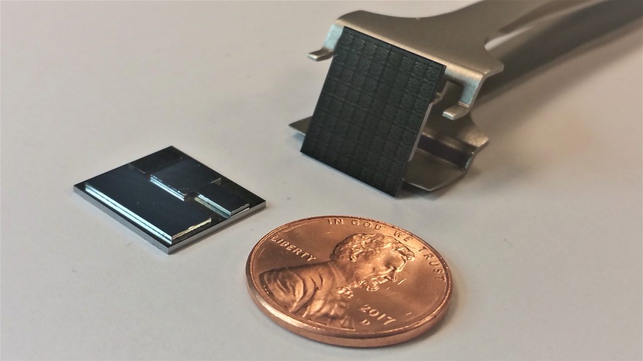
In 2.5 and 3D circuits, one layer typically provides the structural support. Additional layers may be thinned after stacking – sometimes down to mere microns. This means that added layers add almost no bulk to the finished device, as shown by the 2.5D die-on-interposer solution in Figure 2.

The “right” packaging technology is the one that optimizes the product for its intended use. NHanced, with its expertise in advanced packaging, applied materials, chiplets, and heterogeneous integration, stands ready to carry your design to success through this intricate and complex landscape.
Talk to us about your project, and let’s explore how advanced packaging can tailor your next semiconductor solution to your precise needs.


