How a sensor functions is significantly impacted by its packaging technology. Advanced packaging, whether 2.5D or 3D, offers numerous advantages for sensors including:
- 100% fill factor
- 4-side abuttable devices
- Fast local processing
- Optimized process separation
Let’s explore these benefits to understand the choices available and determine when it’s beneficial to adopt 3D packaging technology.
Fill Factor and Device Efficiency
In traditional 2D packaging, sensing elements share the surface with electronics and wiring, which limits the fill factor – the proportion of the device area that is devoted to active sensing elements. A higher fill factor means higher resolution and less “dead space.”
Moving the design to 2.5D or 3D enables the sensing elements to completely fill the outer layer – 100% fill factor – with wiring and electronics hidden below. The entire surface of the device is active.
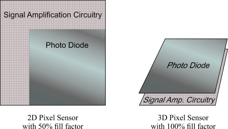
Figure 1: Comparison of 2D and 3D pixel sensors, demonstrating the improved fill factor with 3D packaging.
This configuration ensures the entire surface of the device is active, greatly improving efficiency. For photo sensors, a 100% fill factor eliminates the need for micro-lenses.
Abuttable Devices
Traditional chips communicate along their edges through I/O connections that occupy space and leave gaps between devices in an array.
With 2.5D and 3D designs, I/O connections emerge from the top or bottom, enabling devices in an array to abut each other on all four sides for a continuous, uninterrupted detection surface.
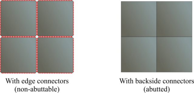
Figure 2: Comparison of abuttable and non-abuttable devices, illustrating an uninterrupted detection surface.
Local Processing
Designing a device in layers makes room for more functionality. “Smart” sensors include logic and memory for local data collection and processing. The sensor can analyze and reduce its data before sending it off-chip, deciding which information merits further attention and which should be simply discarded. This has a host of benefits, including:
- Faster frame rate
- Tight focus on areas of interest
- Reduced data transmission
- Less power consumed; less heat generated
Process Separation
Each component of a 2.5D device and each layer of a 3D device is constructed separately, allowing for process optimization to fine-tune the functionality — detectors with reduced leakage, logic with increased speed, etc. This bespoke build can occur at different nodes, on various wafer types, or even sourced at different foundries. This tremendous versatility – known as heterogeneous integration – is available only with advanced packaging technology.
History and Development of 3D Sensors
The evolution of 3D sensors was initially driven by the demand for back side illuminated sensors. This technology requires extreme thinning of the wafer’s back side, which makes the wafer extremely fragile.
3D wafer stacking solved this problem: the sensor wafer was bonded face-down to an inert wafer. The back of the sensor wafer could then be aggressively thinned without losing structural integrity.
The next advancement was moving the sensors’ support circuitry from the detector wafer to the support wafer. This enabled 100% fill factor on the detector.
Finally, with the advent of through-silicon vias (TSVs) for vertical communication, additional layers were introduced: layers of sophisticated processing logic and sometimes layers of memory. This created “smart sensors” that could collect and process data within a single chip.
Memory layers enable another significant benefit, in that memory consumes less power–and thus generates less heat–than logic. Memory layers are strategically positioned between the sensor and logic layers, effectively dispersing heat, preventing thermal buildup, and illustrating the flexible applications of today’s 3D packaging technologies.
NHanced’s Comprehensive 3D and 2.5D Sensor Solutions
NHanced specializes in building fully customized silicon sensors leveraging 2.5D and 3D packaging technologies. Our processes, tailored at each step, meet precise specifications for prototypes, experimental devices, and small lots.
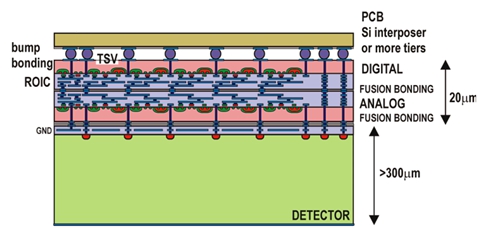
Figure 3: Cutaway diagram of an advanced 3D sensor highlighting the digital ROIC, analog detector, TSVs, and interposer integration.
Our expertise caters to a wide range of applications across industrial, medical, military, and scientific fields, delivering sensors equipped with state-of-the-art features such as:
- Photon imaging chips
- Focal plane arrays (optical, ultraviolet, infrared)
- CMOS image sensors
- CCD full frame sensors
- Particle detector arrays
Our full suite of processing options for 3D and 2.5D sensors includes:
- Wafer coring (resizing)
- Surface planarization
- Back side stress compensation
- Cleaning and deposition
- Tungsten TSV insertion (back side or via-middle)
- Plasma dicing
- Copper and nickel damascene processes and RDL
- Aluminum RDL and pad metal process
We support diverse bonding configurations to suit project-specific needs, including:
- Wafer-to-wafer, die-to-wafer, die-to-die
- Face-to-face, back-to-back, face-to-back
- Chiplet/die/component integration on interposers
- Configurations involving more than three active device wafers per stack
- Low temperature bonding
- Oxide bonding
- DBI® (Direct Bond Integration) hybrid bonding using copper or nickel
- Micro-transfer printing (MTP)
- Thermocompression bonding (TCB)
For back side illumination, our technological capabilities include:
- Silicon thinning: grinding, CMP, dry etch, and wet etch including HNA stop on epi
- IR alignment and printing
- Back side passivation / delta doping / antireflective coating (ARC)
- Back side metal grid
- Back side pad open
For 3D sensor transfer technology, our capabilities further include:
- Temporary bonding and de-bonding
- Oxide bonding and silicon removal, ensuring flexibility and precision in sensor construction.
Interposers play a crucial role in many sensor designs, with options for:
- Thick layer copper damascene
- Silicon, silicon, glass, and organic substrates
- Stitched fields extending up to full wafer scale
At NHanced, our commitment to innovation and quality in advanced packaging solutions for 2.5D and 3D sensors ensures that our clients receive the most advanced, reliable, and tailored sensor technologies available, designed to meet the stringent requirements of today’s diverse application landscape.