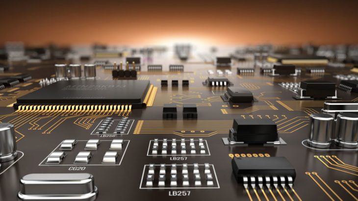
With 2D integrated circuit (IC) technology nearing its scaling limit, there is an urgent need to scale up vertically to cope with the breakneck pace of advances in digital technologies.
2D is old; 2.5D is currently hot; but 3D is the future, according to research analysts Frost & Sullivan. Their report, Future Opportunities for 3D Integrated Circuits, is nicely summarized and discussed in Integrated Circuits get the Third Dimension by P. Nanduri. She notes that high development costs, technical limitations, and a highly unstructured supply chain are limiting the growth of this market. Overcoming the technical limitations is a major focus of SEMI (Semiconductor Equipment and Materials International), a global industry association serving the manufacturing supply chain for semiconductors. A current project is the standardization of Bonded Wafers for Three-Dimensional Integration. Pioneering efforts by Sony, Fermilab, Tezzaron, and others are setting precedents that will enable the next wave of 3D products, inevitably paving the way for even more ambitious endeavors.
3D is the future, and the future looks bright!


